 FARVision
Custom PCB Design
Single and multi-layer PCB design for high-speed, low-power hardware.
What's Included
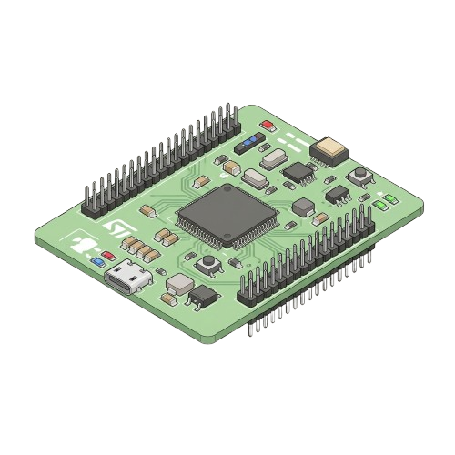
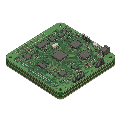
We design custom Printed Circuit Boards built specifically for your product from simple two-layer breakout boards to dense multi-layer boards for high-speed and RF applications. Every layout is engineered for signal integrity, power integrity, and thermal performance. We follow proven design-for-manufacturing (DFM) practices, deliver clean BOMs and Gerbers, and support you through prototype validation and production ramp. Our PCB work pairs tightly with our embedded and firmware teams, so your hardware, software, and manufacturing process are always in sync.
Why Choose This Service
Every engagement is engineered to deliver measurable outcomes not just deliverables.
Precision Layout
Engineered for signal integrity
Low Power
Optimized for efficiency
Manufacturable
Production-ready Gerbers & BOM
A proven process, every time
From your first brief to final handoff, we follow a clear four-step process that keeps you in the loop and the project on track.
Start a ConversationDiscover
We dive deep into your goals, constraints, and success metrics.
Design
We architect the solution and align on scope, timeline, and deliverables.
Develop
Build in focused sprints with regular check-ins and demos.
Deliver
Launch, monitor, and hand over with documentation and support.
Let's Build Something Great
Have a project in mind or want to discuss your Custom PCB Design idea? We'd love to hear from you.